PCB Copper Foils
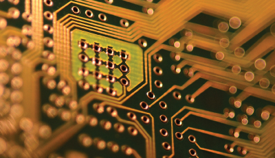
Copper is central to the function of printed circuit boards. The copper traces serve as the primary pathway through which electrical signals travel through the PCB and to mounted components. As such, the thickness of the PCB copper is a critical variable in the board's performance.
PCB copper starts out as a large, uniform foil that is laid directly on the board substrate material. After the foil is bonded to the substrate, the board will undergo an etching process to remove unwanted copper, leaving only the desired trace patterns. There are two primary processes that are used to make these foils, each with their own advantages and disadvantages:
- Electrodeposited (ED) copper: copper ions from an electrolytic solution are deposited onto rotating metal drums, then peeled off in a continuous roll of foil. The resulting foil has vertical grain structure and rough surface, and is typically used in rigid PCBs.
- Rolled annealed (RA) copper: copper billets are pressed by rollers until they are the desired thickness. RA copper foil has a horizontal grain structure and smooth surface with a good degree of flexibility, which makes it good for rigid-flex and flex circuit boards. However, it is considerably more expensive than ED copper.
The copper foils are classified into standard copper ounce weights, which correspond to industry-defined copper thicknesses. Common weights included:
| Cu weight (per square foot) | ½ oz | 1 oz | 2 oz |
|---|---|---|---|
| Thickness (µm) | 18µm | 35µm | 70µm |
1 oz is the most common copper weight used for PCBs, offering a good balance between electrical capabilities, flexibility, etching capability, and cost. While a board using 1 oz will nominally have 35µm of copper thickness, the actual thickness can vary. Additional plating steps in the manufacturing process can further increase copper thickness, while etching and handling can reduce it. As such, having a test method that can accurately and precisely determine copper thickness at different stages – especially one with a smaller spot size to account for small trace width – is a powerful advantage for PCB quality analysis.
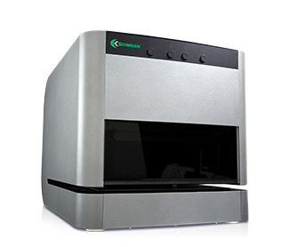
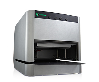
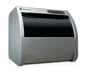
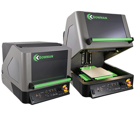
X-Ray Fluorescence (XRF) is a test method that is fast, reliable, and requires little to no sample preparation. Bowman collimated benchtop XRF systems come with multiple collimator options for measuring a variety of trace widths, as well as high-resolution silicon drift detectors (SDDs) for precise measurement of the range of thicknesses typical for 1 oz PCB copper. One of the most critical advantages of XRF is that it is non-destructive, meaning material intended for production can be analyzed directly without being consumed. A single measurement can give manufacturers an accurate Cu thickness within seconds.
To learn more about how you can use x-ray fluorescence to measure copper, read our latest application bulletin!
Conclusion
Bowman B, P, L, and K series are ideal tools for precise measurement of copper. Bowman benchtop XRF systems come with multiple collimator options for measuring a variety of trace widths and a precise XYZ stage for easy programmability to measure multiple points with one click. With a user friendly and feature-rich Archer software, Bowman XRF systems are the ultimate one-stop solution for thickness measurement, elemental and plating bath analysis. Call our support team for more information.

 Made in the USA