Lead frames: the critical link in semiconductor device assembly
Lead frames form the connections between silicon-based integrated circuit devices and printed circuit boards. Semiconductor chips are bonded to the lead frame, which is then packaged as an assembly that is soldered onto a PCB. Metal plating layers are applied to provide corrosion resistance and solderability. The metals chosen are based on the device requirements, and are often a combination of Au, Ag, Pd, and Ni. Newly emerging technologies such as micro-PPF allow specialized platers to provide mass quantities of lead frames to chip manufacturers in a consistent manner.
Lead frames often use precious metals, and it’s important for platers to control the thickness of these expensive materials. Selective plating can minimize metal consumption, but is not always possible depending on the design and the areas requiring plating. Regular XRF testing then becomes a critical factor in maintaining profit margins for lead frame manufacturers.
Bowman systems use silicon drift detector (SDD) technology exclusively for best all-around performance. SDDs offer the best resolution, lowest noise level (highest S/N ratio), long-term stability, and shortest test times. Combined with Bowman’s highly reliable x-ray tube, this hardware duo represents a solid core in every XRF system we manufacture.
As with all electronic devices, lead frames are becoming smaller, so it’s important to accommodate these decreasing feature sizes. This means that the x-ray beam must be small enough to focus on very small areas in order to generate accurate measurements. For this, Bowman offers a broad range of collimator sizes; for very small components, there are several poly-capillary optics options ranging from 7.5-80 µm FWHM. Poly-capillary optics offer not only the smallest x-ray spot size, but also allow for the shortest test times (1-5 s.) In high throughput operations, an optics system can be the workhorse needed for process control and cost minimization.
Bowman offers a range of chassis and sample stage sizes to accommodate a wide variety of part sizes and testing volumes. Many of our customers work with very small parts such as pin connectors, and need to measure many samples per lot of parts to satisfy customer sampling requirements. Often, custom fixtures are used to secure small samples and present them consistently to the XRF system. Multi-point programs can be created, saved, and recalled in order to automate the testing of multiple parts. A programmable XY stage, combined with our built-in pattern recognition software makes high volume testing both efficient and consistent.

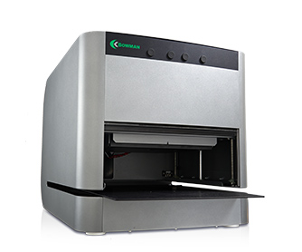
P Series
Sample chamber dimensions 12”x13”x5.5” (WxDxH). Includes programmable XY stage (travel from 5”x6” to 16”x16”) and multiple collimators (4, 8, 12, 24mil default, customized options available). SDD detector standard on both models; large-window SDD optional for fastest test times.

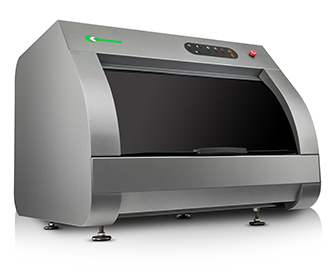
W Series
Sample chamber dimensions 22”x24”x11” (WxDxH). Includes programmable XY stage (travel 10”x10”) and multiple collimators (4, 8, 12, 24mil default, customized options available). SDD detector standard; large-window SDD optional for fastest test times
Need Help? LET’S TALK
Do you need to analyze features less than 

The Bowman O Series XRF delivers small feature analysis with exceptional accuracy; flux density gain up to 5 orders of magnitude compared to collimator. System is equipped with large window SDD.


 Made in the USA