Congrats to Delta Sales

July, 2018 – Delta Sales Associates Inc. announces the recent sale of the Bowman Model “P” XRF plating thickness measurement system to TTM, North Jackson, OH. TTM will use the Bowman system to precisely measure ENIG, ENEPIG, tin lead and other deposits.

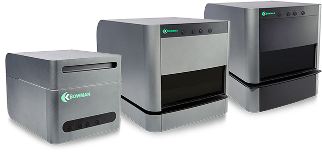
The Bowman Model “P” XRF was engineered specifically for PCB and connector applications; it has an extended table, and is guaranteed IPC 4552 Rev A capable.


Bowman Distributor Moves to New Headquarters

July, 2018 – X-RAY NOW, Bowman’s exclusive distributor and support provider for California, Arizona, Nevada, Colorado, the Pacific Northwest and Mexico, has a new headquarters in Santa Ana, CA. X-RAY NOW has provided XRF coating thickness measurement systems for the PCB and semiconductor industries since 2001. It sells new and used XRF equipment, and provides service, repair and calibrations, and standards, too.

X-RAY NOW offers customer demos for Bowman equipment, either in their facility, or at the customer’s location. You can reach Zach, Phil and their highly experienced XRF team at 714-396-2519.

Bowman Featured at JPCA

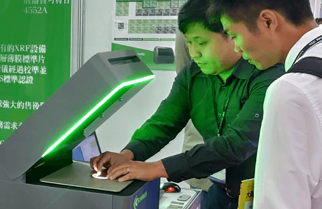
June, 2018 – JPCA (Japan Electronics Packaging and Circuits), was held in Tokyo June 6th through June 9th. Koichiro Hotta and his team at Flex Service Co., Ltd. demonstrated the Bowman P Series at this annual event, which last year drew 43,000+ attendees.


New XRF Instrument Measures the Smallest Features in Semiconductor / Microelectronics Manufacturing

June, 2018 – Bowman, a US manufacturer and global service provider for quality labs using XRF measurement technology, has introduced a new instrument for the smallest features in semiconductors and microelectronics.

Bowman’s W Series uses poly-capillary optics to focus the X-ray beam to 7.5 µm FWHM, the world’s smallest beam size for coating thickness analysis using XRF technology. A 150X magnification camera is used to measure features on that scale; it is accompanied by a secondary, low-magnification camera for live-viewing samples and birds-eye macro-view imaging. Bowman’s dual-camera system lets operators see the entire part, click the image to zoom with the high-mag camera, and pinpoint the feature to be programmed and measured.

A programmable X-Y stage with precision less than +/- 1 µm for each axis is used to select and measure multiple points; Bowman pattern recognition software and auto-focus features also do this automatically. The system’s 3D mapping capability can be used to view the topography of a coating on a part such as a silicon wafer.