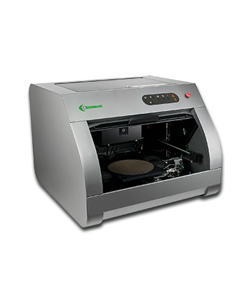
June, 2018 – Bowman, a US manufacturer and global service provider for quality labs using XRF measurement technology, has introduced a new instrument for the smallest features in semiconductors and microelectronics.
Bowman’s W Series uses poly-capillary optics to focus the X-ray beam to 7.5 µm FWHM, the world’s smallest beam size for coating thickness analysis using XRF technology. A 150X magnification camera is used to measure features on that scale; it is accompanied by a secondary, low-magnification camera for live-viewing samples and birds-eye macro-view imaging. Bowman’s dual-camera system lets operators see the entire part, click the image to zoom with the high-mag camera, and pinpoint the feature to be programmed and measured.
A programmable X-Y stage with precision less than +/- 1 µm for each axis is used to select and measure multiple points; Bowman pattern recognition software and auto-focus features also do this automatically. The system’s 3D mapping capability can be used to view the topography of a coating on a part such as a silicon wafer.

 Made in the USA