Advantages of Polycapillary Optics for Semiconductors
The semiconductor industry plays an instrumental role in powering and advancing modern technology,
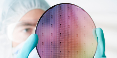
touching all industries from consumer electronics like computers and phones, to medical, automotive, communications, energy, defense, and AI. The demand for smaller, faster, more advance and cost-effective products has led to rapidly evolving material usage and increasingly shrinking feature sizes. As the industry continues to innovate, it is important to accurately monitor material thickness and composition in a non-destructive manner to ensure quality and efficiency throughout the manufacturing process.
The mechanical properties of a semiconductor heavily depend on precise material deposition, integration, and packaging. At all stages, it is critical to monitor both thickness and composition of the material used. High lead concentrations in tin-lead (SnPb) solders can lead to brittle joints and low mechanical strength, while low concentrations run the risk of tin whiskers, resulting in subsequent short circuits. Low palladium thickness in ENEPIG surface finishes compromises the diffusion barrier and allows for potential nickel corrosion, however overplating wastes expensive material. Other common metals such as copper (Cu), aluminum (Al), and titanium (Ti) also jeopardize semiconductor integrity when improperly plated. Increased resistance, heat dissipation complications, weak connections, and other potential issues all pose significant risks to semiconductor performance.
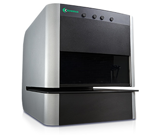
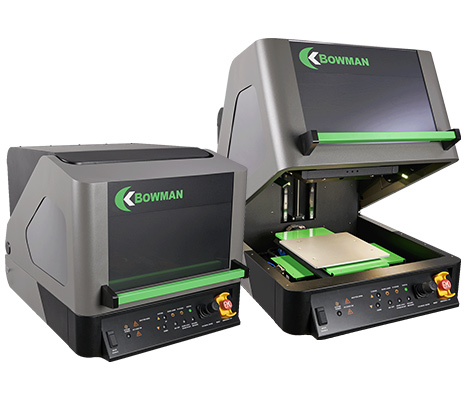
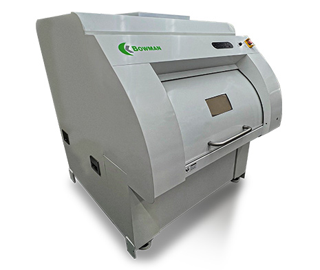
The Bowman polycapillary optics systems are specifically designed to meet and exceed quality expectations of the semiconductor industry. In addition to the ability to measure down to 15µm/7.5µm FWHM spot size, Bowman systems also come equipped with state-of-the-art Large Window Silicon Drift Detectors and customizable tube targets to optimize unique application performance. The dual camera system includes a 140x micro-viewing camera (with 7x digital zoom) and a 9x macro-viewing camera, allowing users to toggle between the low magnification camera to see a wider view of the sample and the high mag. camera to precisely pin-point small features. Additionally, the Table View feature allows for capturing an image of the entire XY stage and using point-and-click to automatically move the sample features under the micro camera. A high-precision stage coupled with advance pattern matching software ensures users can easily and repeatably analyze samples at the correct measurement locations. The M, K, W, and A series all outperform the requirements of IPC-4552, 4553, 4554, and 4556, and conform to ASTM B568 and ISO 3497. Moreover, all of these systems can also be integrated into an automated in-line inspection line. Read more about hardware and software advantages of Bowman Optics systems for semiconductors here: https://bowmanxrf.com/semiconductors-wafers/
Read our latest application note on Semiconductor Applications performance to see the proof!
Conclusion
Bowman polycapillary optics systems are versatile and non-destructive analytical tools for quickly and preciously measuring critical semiconductors applications. Bowman XRF serves as an all in one instrument for measuring up to 5 layers and 30 elements of plating thickness and composition, as well as single and multi element solution analysis. the M, K, W, and A series are engineered for the work environments of the wafer/packaging industries with a broad range of chassis sizes, sample stage size and travel, x-ray spot size, and video cameras. It comes with an easy to use and feature-rich software with customizable data storage and management. Call our support team for more information.

 Made in the USA